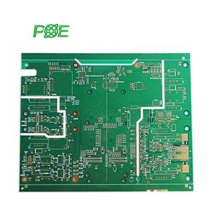
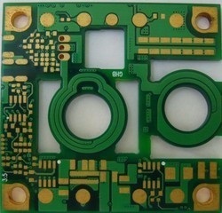
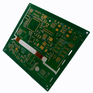
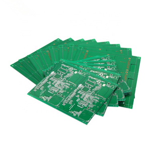
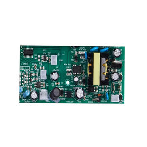
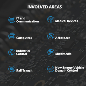
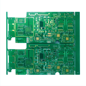
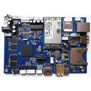
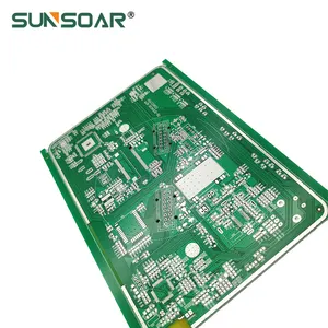
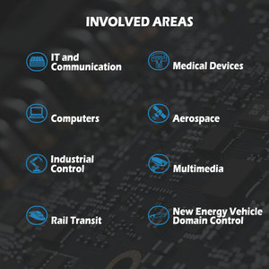
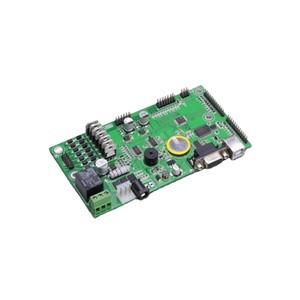
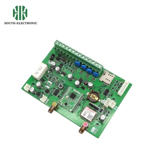
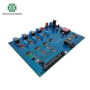
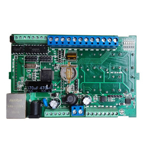
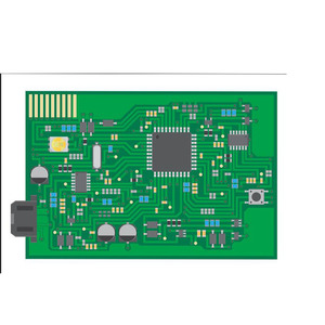
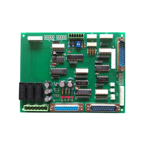
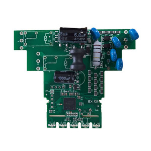
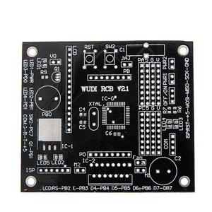
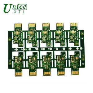
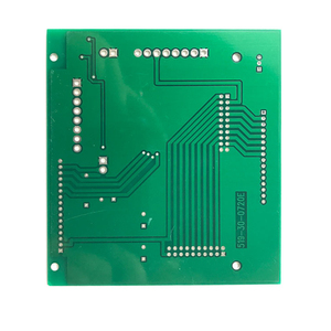
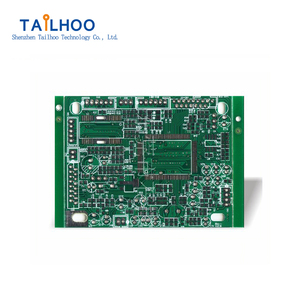
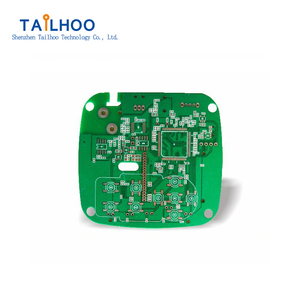
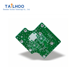
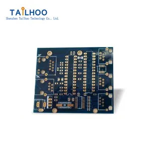
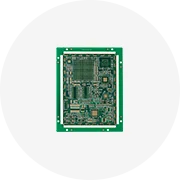
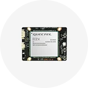
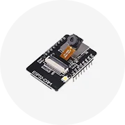
The 10 layer pcb term is important in the construction and manufacturing of electronic devices. These devices have components on a printed circuit board (PCB), which are very important in today's electronics, enabling complex functions and connections. 10 layer pcb is used in various industries, such as telecommunications, automotive, consumer electronics, and medical devices. They integrate many electronic components into a neat and efficient package, thereby becoming inseparable in the production of cutting-edge technology. As electronic devices develop, innovative, high-performance 10 layer pcb is increasingly needed, and this results in advancements in design and manufacturing processes.
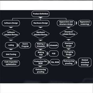
Types of 10 layer pcb
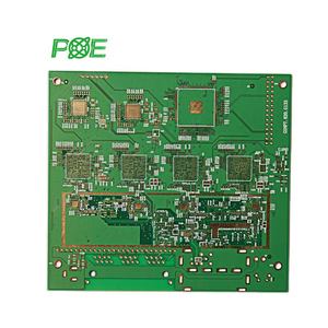
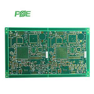
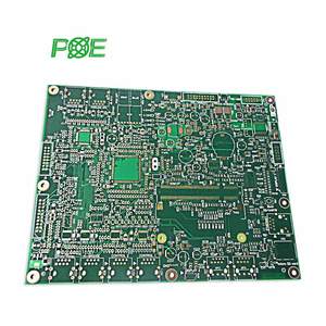
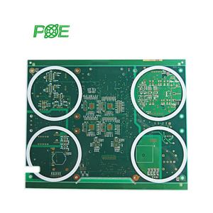
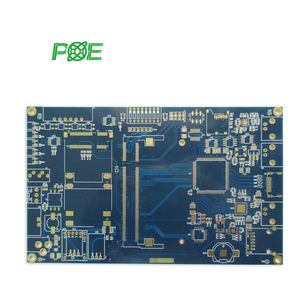
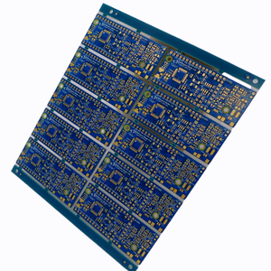
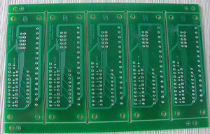
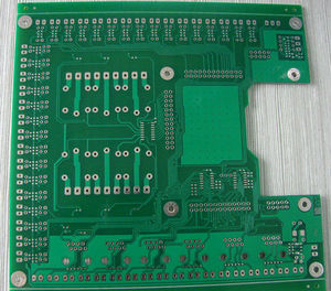
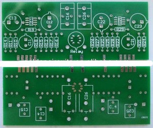
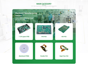
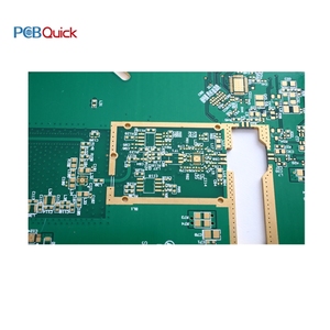
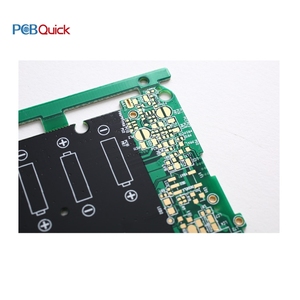
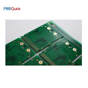
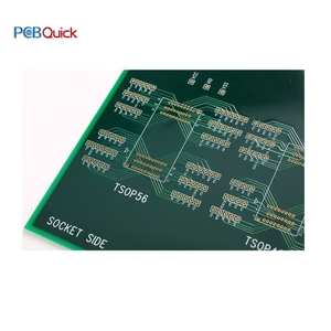
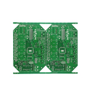
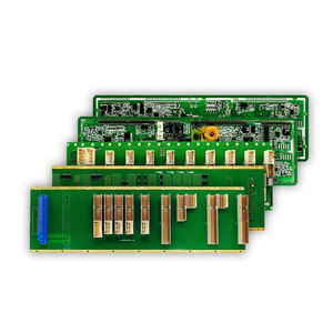
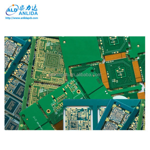
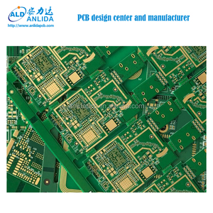
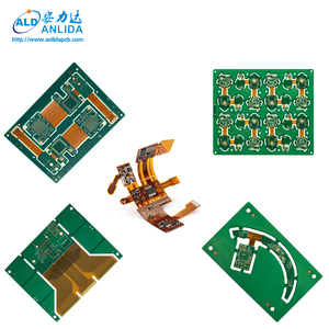
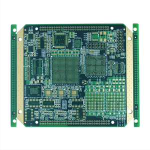
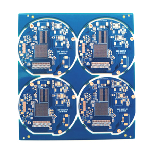
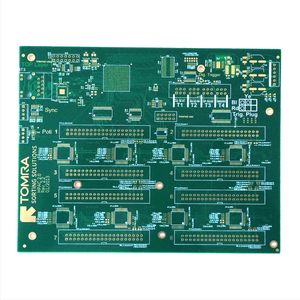
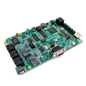
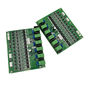
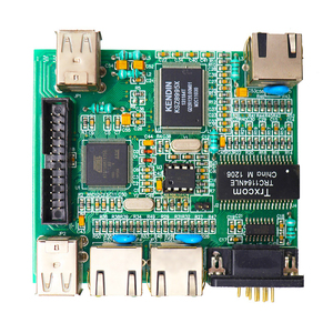
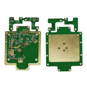
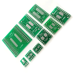
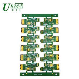
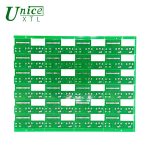
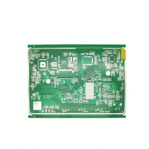
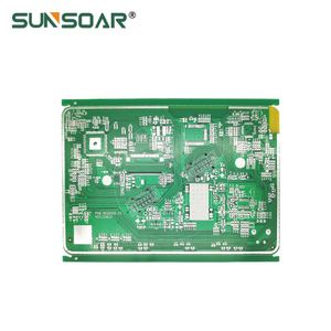
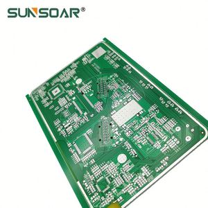
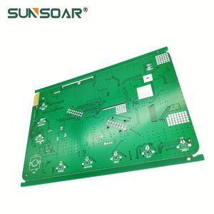
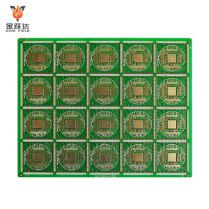
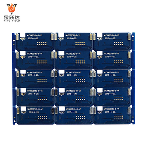
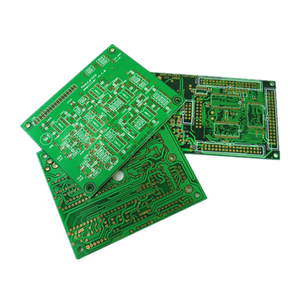
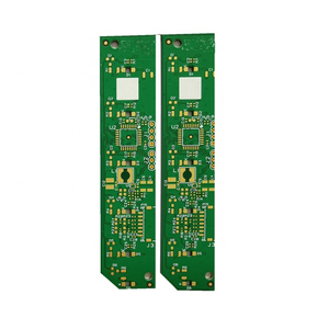
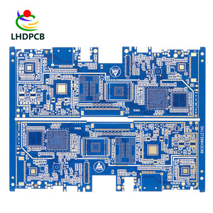
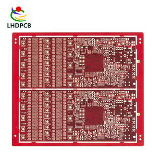
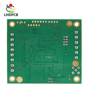
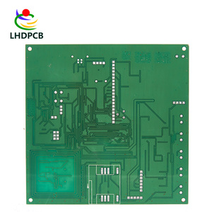
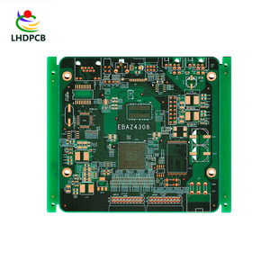
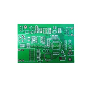
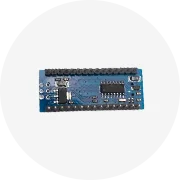
There are a number of 10 layer pcb types to meet individual application requirements: single-sided, double-sided, and multi-layer assemblies. Single-sided assemblies contain components on one side of the PCB and are applied in less complex electronics. Double-sided assemblies permit components on both sides, with increased complexity and functionality. Multi-layer assemblies combine several layers of PCBs with increased density and more complex circuits. Each type of 10 layer pcb has its own advantages so that designers can choose the most suitable configuration for them.
Functions and Features of 10 layer pcb
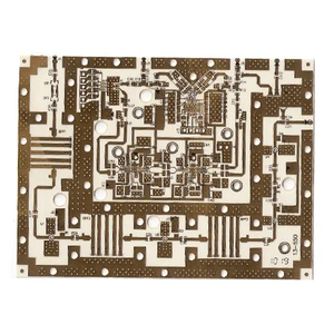
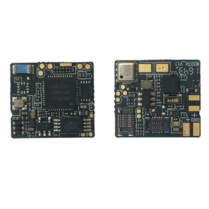
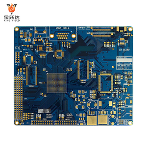
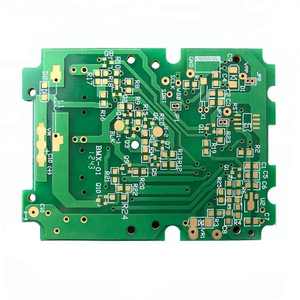
The main function of 10 layer pcb is to enable the interaction and communication between electronic components within a device. Pathways for conducting on PCB enable efficient transmission of electrical signals. The most unique features of 10 layer pcb are small size, reliability, and high-speed data transfer. They are made to work under different conditions of the environment to ensure longevity and durability. Advanced 10 layer pcb possess extra capabilities such as thermal control and electromagnetic interference shielding, which enhance their performance in harsh environments.
Materials and Ingredients Utilized in 10 layer pcb
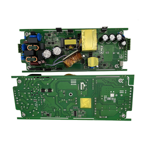
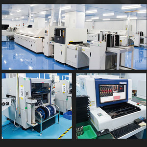
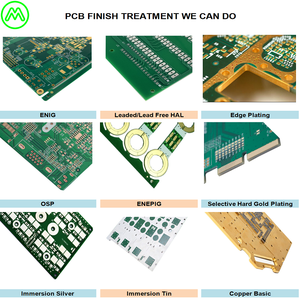
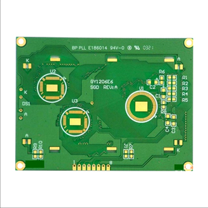
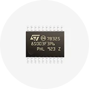
Production of 10 layer pcb entails various materials for performance and durability. The most critical material is the substrate, usually made of a fiberglass-reinforced epoxy resin called FR-4, which serves as mechanical support and insulation. Conductive layers, like copper, are etched on the substrate to form circuit paths. Solder paste and adhesives secure components and offer stable electrical connections. Material selection affects thermal conductivity, electrical performance, and overall reliability of the 10 layer pcb.
How to Utilize 10 layer pcb Efficiently
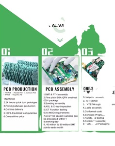
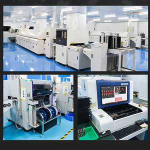
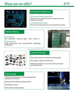
To utilize 10 layer pcb efficiently, take into account the individual needs of the electronic device. Choose the proper assembly type, check compatibility with the device component parts, and adhere to industry standards for manufacturing and design. Proper mounting and handling are most important to maintaining the 10 layer pcb in its optimal working condition, as inefficient procedures could lead to failure or damage. Regular testing and inspection can identify any defect early enough to maintain peak performance. Understanding 10 layer pcb strengths and weaknesses will enable manufacturers to best utilize their strengths and provide quality electronic products.
Choosing the Correct 10 layer pcb for a Project
Selecting the appropriate 10 layer pcb requires primary considerations. Initially, consider the level of complexity of the electronic device. Based on its demands, one might require single-sided, double-sided, or multi-layer 10 layer pcb. Each provides varying degrees of component density and circuit complexity. Further, the thermal performance and endurance needed for the application must be considered since these determine the material and design.
It's also important to ensure that the
10 layer pcb is compatible with the device parts. Make sure that the assembly supports the size, weight, and electrical requirements of all the parts. This involves checking that connections are aligned and that the
10 layer pcb supports the necessary power and data transmission speeds. Knowing the technical specifications ensures that the
10 layer pcb enhances the performance and reliability of the electronic device.
Q&A
What are the advantages of possessing a multi-layer 10 layer pcb?
Utilization of a multi-layer 10 layer pcb can be very beneficial. They provide more circuit density and can handle more complex electronic designs. Multi-layer 10 layer pcb, with multiple signal paths, can enhance the performance of devices as well as reduce interference. They also offer enhanced thermal management along with improved structural strength, which is ideal for high-end applications.
How does substrate material choice impact 10 layer pcb performance?
The substrate material is crucial to the functionality of a 10 layer pcb. Generally available materials like FR-4 offer superior insulation and mechanical rigidity, therefore their common use. In cases where the usage intended requires greater conduction of heat, substrates with more heat conduction capacity, such as ceramic or metal-core substrates, may be appropriate. The choice of substrate material dictates the thermal, electrical, and mechanical stresses a 10 layer pcb can conduct.
What testing procedures are crucial to ensuring 10 layer pcbquality?
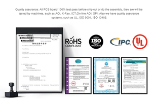
Ensuring the quality of a 10 layer pcb involves several important test procedures. Conduct electrical tests to confirm signal integrity and connectivity and thermal tests to quantify heat dissipation. Mechanical tests can also be utilized to test how rugged the 10 layer pcb is when put under stress. Also, inspecting for defects like solder joint quality and alignment is extremely crucial. These detailed tests can identify possible issues early, ensuring the 10 layer pcb works reliably in the final product.
Can 10 layer pcb be tailored to specific uses?
Yes, 10 layer pcb can be tailored for specific needs and uses. Tailoring may involve a change in the size, form, and layer structure of the assembly or the inclusion of specialty parts. The tailoring ensures high performance and function to fit the specific needs of specific electronic equipment.
What are the environmental impacts of throwing away 10 layer pcb?
In disposing of 10 layer pcb, environmental concerns must be taken into consideration. The majority of assemblies contain materials such as lead and other harmful chemicals that must be disposed of with care. Recycling programs can reclaim valuable materials such as copper and conserve waste. Complying with regulations and standards for electronic waste disposal is essential to minimize environmental harm and encourage sustainability.


 浙公网安备 33010002000092号
 浙B2-20120091-4