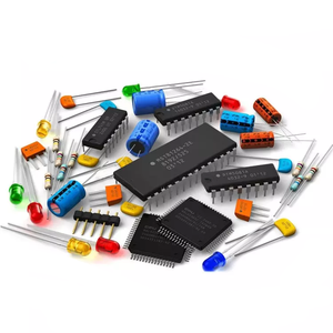
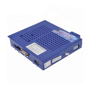
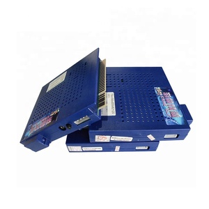
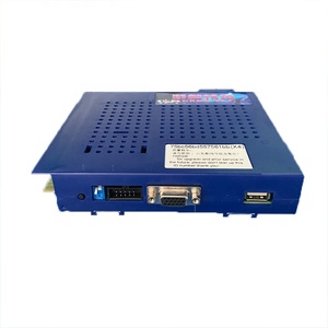
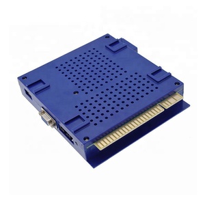
Introduction to Jammer PCB
A jammer PCB (Printed Circuit Board) is a critical component in the design and manufacturing of jamming devices used for disrupting communication signals. These boards are engineered to be efficient and effective in two primary domains: military applications and private sector uses. The complexity of jammer PCBs comes from their need to operate seamlessly within various frequency bands while maintaining functionality and reliability. By using the latest technology, manufacturers can produce highly specialized PCBs tailored to specific jamming requirements.
Types of Jammer PCB
Jammer PCBs can be classified based on their applications and functionalities. Understanding the various types helps users choose the right jammer PCB for their needs:
- Signal Jammer PCBs: Designed specifically to disrupt radio, Wi-Fi, and cellular signals.
- GPS Jammer PCBs: Focus on interfering with GPS signals to provide stealth capabilities.
- Wi-Fi Jammer PCBs: Target Wi-Fi networks, often used in areas with high density of devices.
- Two-way Radio Jammer PCBs: Cater to communication between police and other agencies, disrupting their channels.
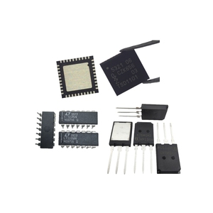
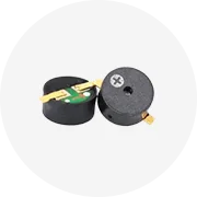
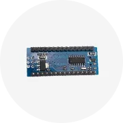
Function, Feature and Design of Jammer PCB
Understanding the function and design of a jammer PCB is vital for effective application. These boards are characterized by several key features:
- Frequency Range: Various jammer PCBs cover different frequency bands, making them versatile in different environments.
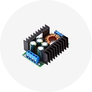
- Power Output: Power output capabilities are crucial; high wattage offers stronger jamming potential.
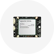
- Small Form Factor: Modern designs emphasize compactness, allowing for easy integration into portable devices.
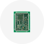
- Durability: Jammer PCBs are manufactured using robust materials to ensure resilience under diverse operating conditions.
- Cooling Mechanisms: Incorporation of heat sinks or thermal management systems prevents overheating during prolonged operation.
Applications and Advantages of Jammer PCB
The utility of jammer PCB extends across various fields, thanks to its unique capabilities. Here are the notable applications and advantages:
- Military Operations: Essential for ensuring communication security by disrupting enemy signals.
- Private Security: Used in secure facilities to prevent unauthorized communications and protect sensitive information.
- Event Management: Implemented during high-profile events to prevent potential threats by disabling nearby devices.
- Research and Development: Vital in testing and development of communication systems, allowing engineers to analyze signal vulnerabilities.
Additionally, the advantages of jammer PCBs include:
- Enhanced security through signal disruption, ensuring that unauthorized communications are thwarted.
- Cost-effectiveness by reducing the need for additional security measures.
- Improved reliability with consistent operation that meets professional standards.


 浙公网安备 33010002000092号
 浙B2-20120091-4